Pokémon mini Development Documentation
Cartridge
For the cartridge header used for software, see here
A commercial Pokémon mini cartridge is a 512 KiB ROM with a staggered 32-pin connector. The pins as well as an unnecessary border around the top have an ENIG finish.
To open the case, there are two Y1 tri-wing screws on the back. Once removed, slide the front half of the case downward then it’s free to remove. The board will just fall out.
When in its case, much of the front of the board is covered by the sticker; only the ROM chip is visible. The back is in full view, and is a silk-screen containing a logo, copyright, and cartridge code: MIN-KCM1-01.
TODO: board scans
The board is approximately:
- Width: 27.7 mm (generally)
- Screw hole cutouts diameter: 4.5 mm
- Height: 23 mm
- Thickness: 1 mm thick
Shells
The ornamental design patent is USD478127.
The case is approximately:
- Width: 33.5 mm
- Height: 26.5 mm (back), 33 mm (arc of the rounded part)
- Thickness: 1 mm (most of the plastic), 5.1 mm (back to sticker), 8.2 mm (thickest)
There are a handful of shell designs which fit commercial game PCBs and flash carts which are compatible with it.
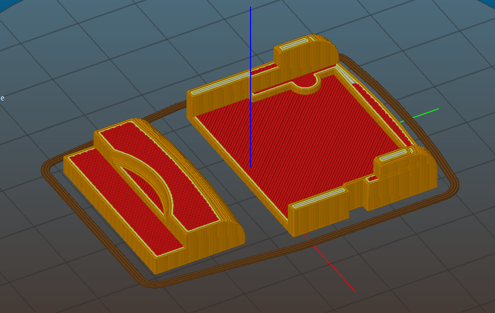
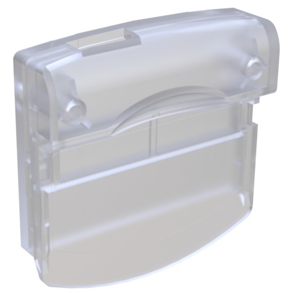
- By Ksanto, designed for DITTO mini but also works for PokeCard 512 rev 2+
- Based on Ksanto’s, by 4thAxisDesign, offers a version with a hole (positioned for the PokeCard 512 rev 2+ and DITTO mini) and one without, as well as using the notch on the bottom shell by AlexiG to support the PokMini PCBs.
- By cyborg_ar which was intended for DITTO mini but never got a hole. STLs were never released nor was the shell finished.
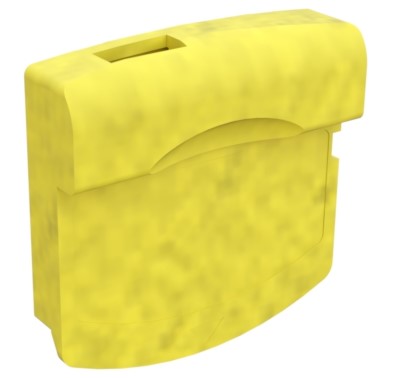
- By Pikpol, also in yellow, which was intended for DITTO mini. STLs were never released.
Using this document
On this board, all chips are on one side. We describe locations using the following abbreviations: top-left (TL), top-right (TR), middle-left (ML), middle-right (MR), bottom-left (BL), and bottom-right (BR).
For our purposes, bottom refers to where the pins are, such that CN1 can be read correctly.
Legend
The purpose of the circled I mark is possibly the board manufacturer.
There’s a single digit printed on the right side, above B1, with unclear purpose. On my JP Party mini it’s a 6. Possibly a 1-digit serial.
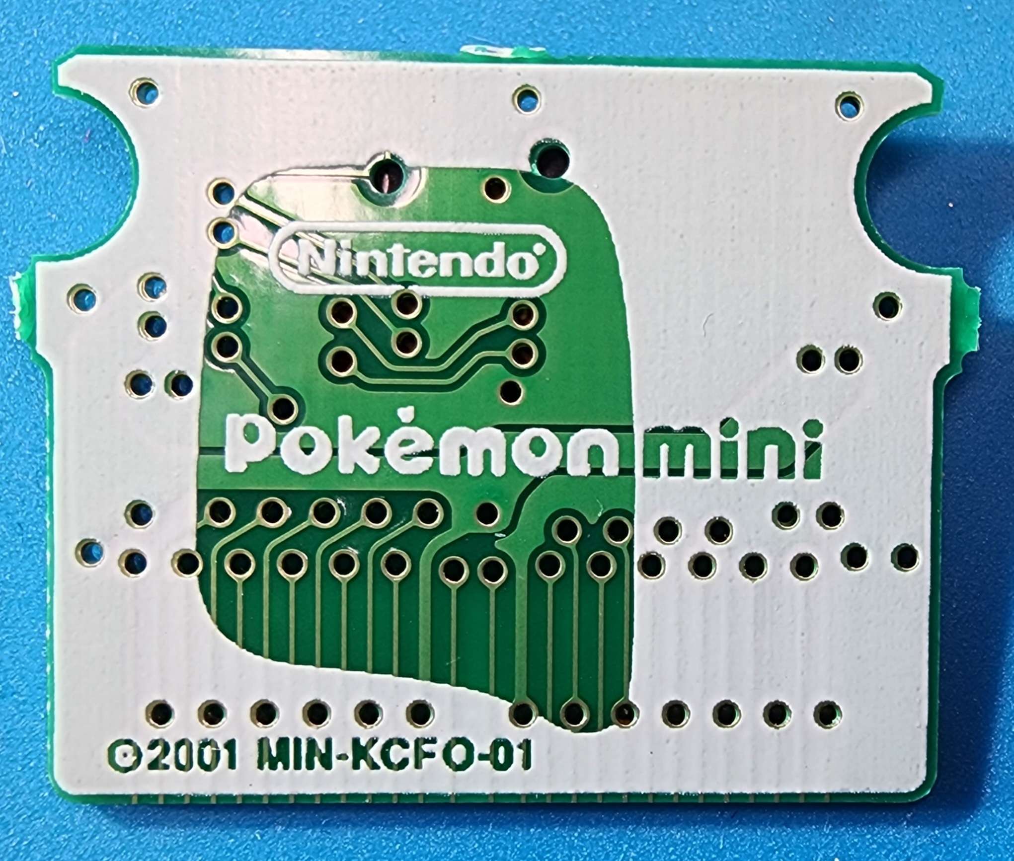
An M 1 is printed between the CN1 text and the pins, which is possibly the board revision, as the sample cart has F 0 here instead. This is from the code printed on the back, MIN-KCM1-01 or MIN-KCF0-01.
There is a 01 printed under the TSOP diagram which likely reflects the 01 from the product code printed on the back (MIN-KCM1-01). It does not appear to be a board revision as the sample cart, which has a different layout, also uses 01. It’s possible that it refers to the year, 2001. However, no 02 release is known.
There is a graphic masked onto the board which looks like a rectangle with 0 or more dots inside and the corners marked 1 (TL), 6 (TR), 7 (BL), 12 (BR). It does not correspond with the ROM pins and is unclear what else it might refer to.
- C - Capacitor
- CN - Connector
- R - Resistor
- U - Unit: ROM
Capacitors
All capacitors are surface mounted (SMD) multilayer ceramic capacitors (MLCC).
| Label | Populated? | Location | Capacitance |
|---|---|---|---|
| C1 | yes | MR, left of C3 | ? |
| C2 | yes | middle | ? |
| C3 | yes | MR | ? |
| C4 | yes | ML | ? |
CN1
This refers to the pins. The top row is labeled B1 (on the right) and B17 (on the left). The community has had two methods of referring to the other row of pins: the right-most being either B1.5 or A1. Here, we prefer A1.
The pitch between two pins on the same row is 1 mm, making the pitch between two pins on opposite rows 0.5 mm. B1 and B17 are shaped like MissingNo. All the A pins are rounded on top and have through-holes on the top, they are slightly taller and narrower than the B pins. All the B pins except 1, 16, and 17 are rounded on top and have traces connecting upward. B16 is rectangular, but otherwise the same dimensions as the other B pins.
Pin A1 is attached to the large B1 contact and pin A16 is attached to the large B17 contact.
I/O listed from the perspective of [U1][]. PS = Power Supply.
TODO: confirm voltage, is it really 3.3v ??
| Contact | CN4 pin | Name | I/O | Description |
|---|---|---|---|---|
| B1 | 1 | VDD | PS | Stepped down from VCC |
| A1 | 2 | VDD | PS | Stepped down from VCC |
| B2 | 3 | A20 | I | Address bit 20 |
| A2 | 4 | A9 | I | Address bit 9 when LALE=high, 19 when HALE=high |
| B3 | 5 | A8 | I | Address bit 8 when LALE=high, 18 when HALE=high |
| A3 | 6 | A7 | I | Address bit 7 when LALE=high, 17 when HALE=high |
| B4 | 7 | A6 | I | Address bit 6 when LALE=high, 16 when HALE=high |
| A4 | 8 | A5 | I | Address bit 5 when LALE=high, 15 when HALE=high |
| B5 | 9 | A4 | I | Address bit 4 when LALE=high, 14 when HALE=high |
| A5 | 10 | A3 | I | Address bit 3 when LALE=high, 13 when HALE=high |
| B6 | 11 | A2 | I | Address bit 2 when LALE=high, 12 when HALE=high |
| A6 | 12 | A1 | I | Address bit 1 when LALE=high, 11 when HALE=high |
| B7 | 13 | A0 | I | Address bit 0 when LALE=high, 10 when HALE=high |
| A7 | 14 | VDD | PS | Stepped down from VCC |
| B8 | 15 | HALE | I | High address bits are latched when HALE is high |
| A8 | 16 | - | - | No pad |
| B9 | 17 | LALE | I | Low address bits are latched when LALE is high |
| A9 | 18 | GND | PS | Ground |
| B10 | 19 | D0 | I/O | Data bit 0 |
| A10 | 20 | D1 | I/O | Data bit 1 |
| B11 | 21 | D2 | I/O | Data bit 2 |
| A11 | 22 | D3 | I/O | Data bit 3 |
| B12 | 23 | D4 | I/O | Data bit 4 |
| A12 | 24 | D5 | I/O | Data bit 5 |
| B13 | 25 | D6 | I/O | Data bit 6 |
| A13 | 26 | D7 | I/O | Data bit 7 |
| B14 | 27 | OE | I | Output Enable. CPU reading data when OE is high |
| A14 | 28 | IRQ | O | Causes [Cartridge IRQ][] when IRQ is high |
| B15 | 29 | WE | I | Write Enable |
| A15 | 30 | CS | I | Chip Select |
| B16 | 31 | CARD_N | O | Card detect. Active-low. Connected to GND |
| A16 | 32 | GND | PS | Ground |
| B17 | 33 | GND | PS | Ground |
Resistors
| Label | Populated? | Location | Resistance |
|---|---|---|---|
| R1 | yes | ML, right of C1 | ? |
| R2 | yes | ML, right of R1 | ? |
U1
On commercial ROMs this is a MX23L4004-12A mask ROM chip. It’s a 32-TSOP, 20 mm wide x 8 mm tall.
Seemingly no other Macronix chip uses this address demuxing scheme and the datasheet is not available.
- MX - Manufacturer (Macronix International Co., Ltd.)
- 23 - Type: Mask ROM
- L - Voltage: 2.7 ~ 3.6V
- 4 - Density: 4 Megabit (512 KiB)
- 004 - Options?? at least indicates 32-pin somehow
- 12 - Speed?: 120ns??
- A - Parallel
Pins
There is a dot marking pin 1 on the ROM chip itself, and an arrow pointing to it on the board. It’s located at the bottom-right of the chip.
Presumably pins 1 and 24 are the real power supply pins, unclear what the rest are doing. At most, other Macronix ROMs from around this time have two VSS pins, meaning either 13 or 16 might be real too.
I/O listed from the perspective of the ROM. PS = Power Supply.
| Pin # | Name | I/O | Description |
|---|---|---|---|
| 1 | VCC | PS | Power supply pin |
| 2 | A20 | I | Address input bit 20 |
| 3 | A9/A19 | I | Address input bit 9/19 |
| 4 | A8/A18 | I | Address input bit 8/18 |
| 5 | A7/A17 | I | Address input bit 7/17 |
| 6 | A6/A16 | I | Address input bit 6/16 |
| 7 | A5/A15 | I | Address input bit 5/15 |
| 8 | A4/A14 | I | Address input bit 4/14 |
| 9 | A3/A13 | I | Address input bit 3/13 |
| 10 | A2/A12 | I | Address input bit 2/12 |
| 11 | A1/A11 | I | Address input bit 1/11 |
| 12 | A0/A10 | I | Address input bit 0/10 |
| 13 | VSS | PS | Ground pin |
| 14 | HALE | I | High Address Latch Enable |
| 15 | LALE | I | Low Address Latch Enable |
| 16 | VSS | PS | Ground pin |
| 17 | VSS | PS | Ground pin |
| 18 | CE | I | Chip Enable |
| 19 | WE | I | Probably not connected |
| 20 | OE | I | Output Enable input |
| 21 | VCC | I | Power supply pin |
| 22 | D7 | O | Data output bit 7 |
| 23 | D6 | O | Data output bit 6 |
| 24 | VSS | PS | Ground pin |
| 25 | D5 | O | Data output bit 5 |
| 26 | D4 | O | Data output bit 4 |
| 27 | D3 | O | Data output bit 3 |
| 28 | VCC | I | Power supply pin |
| 29 | D2 | O | Data output bit 2 |
| 30 | D1 | O | Data output bit 1 |
| 31 | D0 | O | Data output bit 0 |
| 32 | VCC | I | Power supply pin |
Sample cartridge
The sample cart is a flash cartridge distributed to (likely) reporters in Japan at the time. One sample cart (00954) has been dumped, which contained the full release version of Pokémon Party mini (JP). However the chip is 2 MiB and it has not had the full memory dumped.
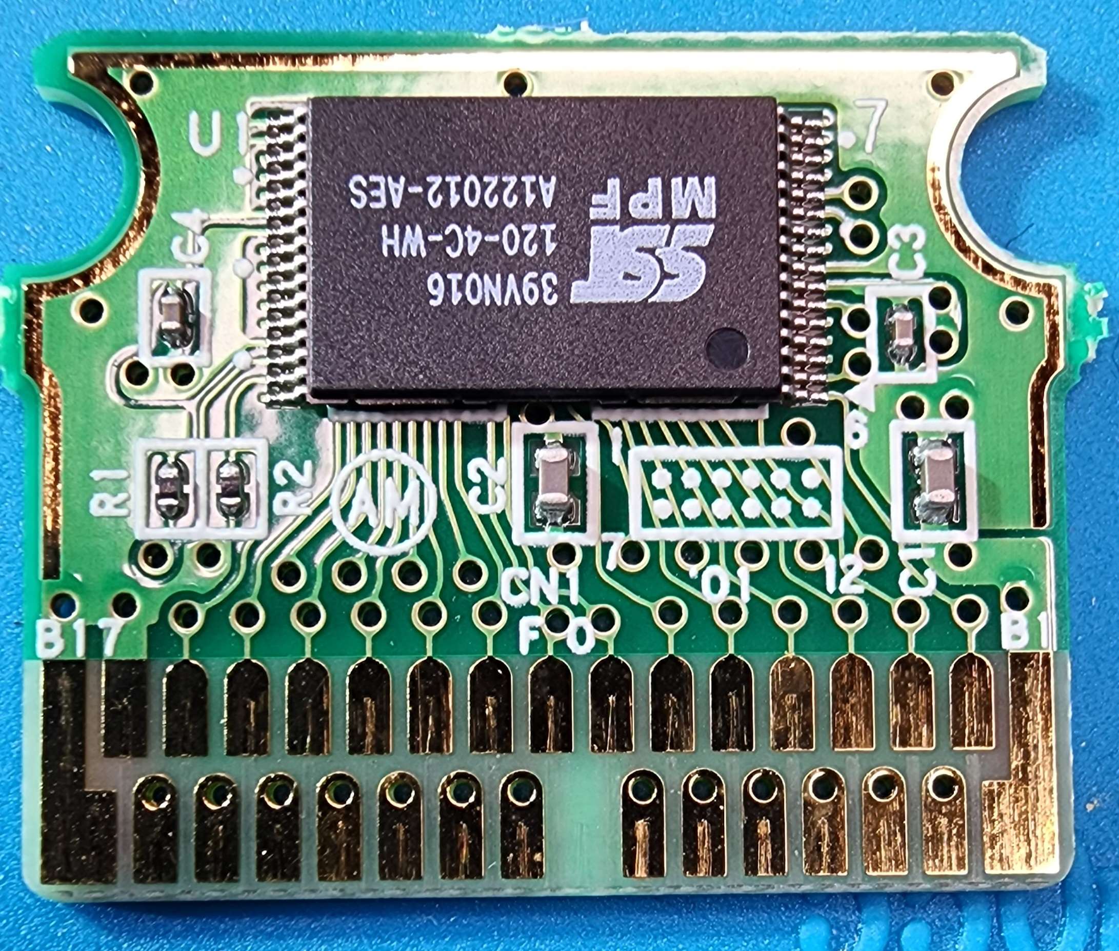
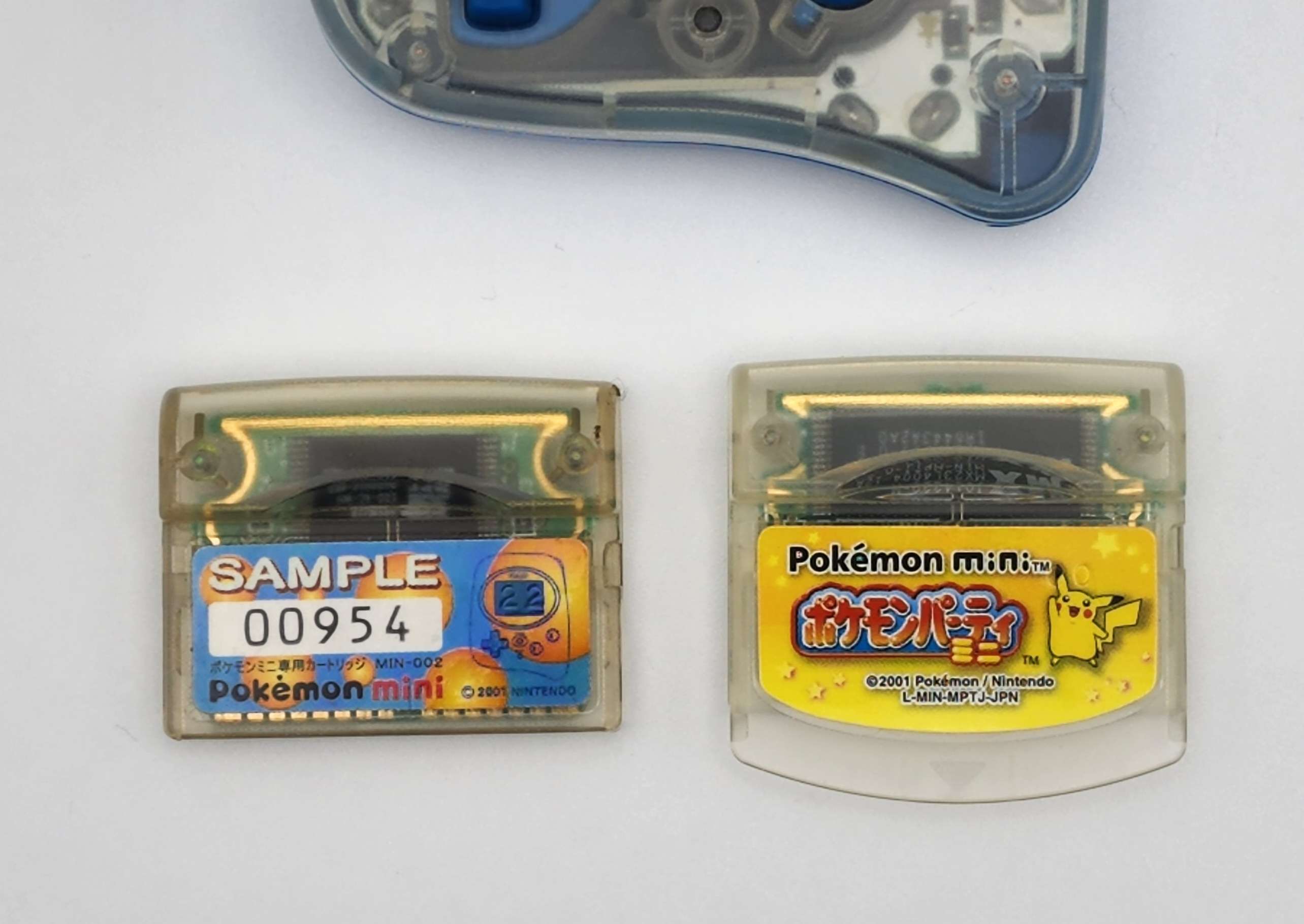
The label on the cart says:
- SAMPLE
- 00954
- ポケモンミニ専用カートリッジ MIN-002
- T/L: Pokémon mini Sample Cartridge
- Pokémon mini
- In the PM: 22
- © 2001 NINTENDO
The back silk-screen has a nintendo logo at the top on the console shape, a different font for the Pokémon mini text, and MIN-KCFO-01 next to the copyright where “Nintendo” would be on commercial carts.
The layout of the components is different, presumably due to the different width of U1. But they do seem to be the same components.
| Component | Location |
|---|---|
| C1 | MR |
| C2 | middle |
| C3 | TR, above C1 |
| C4 | TL, above R1 |
| R1 | ML |
| R2 | ML, right of R1 |
U1
This is a SST39VN016-120-4C-WH flash chip which is a 32-pin version of the typically 40-pin SST39VF016. However it should be software compatible, so even if the BIOS does not refer to this chip, it should be mostly compatible with its dev cart functions.
- SST - Manufacturer (Silicon Storage Technology, Inc.)
- 39 - Product Series: Multi-Purpose Flash
- V - 2.7-3.6V
- N - ???
- 016 - Device Density: 16 Megabit (2 MiB)
- 120 - Read Access Speed: 120 ns
- 4 - Minimum Endurance: 10,000 cycles
- C - Temperature Range: Commercial (0⁰C to +70⁰C)
- W - Package Type: TSOP
- H - Package Modifier: 32 leads
Pins
Due to the expensive nature of this item, the board should not be disassembled, and the exact trace and pinout will likely remain unknown.
The chip has a dot indicating pin 1 and an arrow on the board, same as commercial boards.
| Pin # | Name | I/O | Description |
|---|---|---|---|
| 1 | A20 | I | Address input bit 20 |
| 2 | A9/A19 | I | Address input bit 9/19 |
| 3 | ? | ? | |
| 4 | ? | ? | |
| 5 | ? | ? | |
| 6 | ? | ? | |
| 7 | VDD | PS | Power supply pin |
| 8 | VSS | PS | Ground pin |
| 9 | ? | ? | |
| 10 | ? | ? | |
| 11 | ? | ? | |
| 12 | ? | ? | |
| 13 | ? | ? | |
| 14 | ? | ? | |
| 15 | ? | ? | |
| 16 | ? | ? | |
| 17 | VSS | PS | Ground pin |
| 18 | VSS | PS | Ground pin |
| 19 | ? | ? | |
| 20 | ? | ? | |
| 21 | ? | ? | |
| 22 | VSS | PS | Data output bit 7 |
| 23 | VDD | PS | Power supply pin |
| 24 | ? | ? | |
| 25 | ? | ? | |
| 26 | ? | ? | |
| 27 | ? | ? | |
| 28 | ? | ? | |
| 29 | VDD | PS | Power supply pin |
| 30 | ? | ? | |
| 31 | ? | ? | |
| 32 | ? | ? |
My JP Party mini markings
- On the inside face of the front part, each in rectangles: F >ABS< 1-8
- On the inside face of the back part, each in rectangles: B >ABS< 1-4
- On the outside face of the back, centered in a square:
- Nintendo logo
- MODEL NO.
- MIN-002
- PAT. PEND.
- MADE IN JAPAN
- The rectangle: two circles in the bottom right of it
- Above B1: 6
- Under CN1: M 1
- Right of CN1: 01
- Back: ©2001 Nintendo MIN-KCM1-01
- There are two circles on the edge of the right screw hole cutout and half of one on the left’s
- U1, 4 lines:
- J014220-M
- MX23L4004-12A
- MIN-MPTJ-0 E
- 1R6601A1